Patterned Wafer Inspection System

5 Wafer Defect Inspection System Hitachi High Tech Global

Patterned Wafer Inspection

Semiconductor Wafer Defect Inspection Reliant Systems Inc

Optical Patterned Wafer Inspection Tool Market To Escalate News

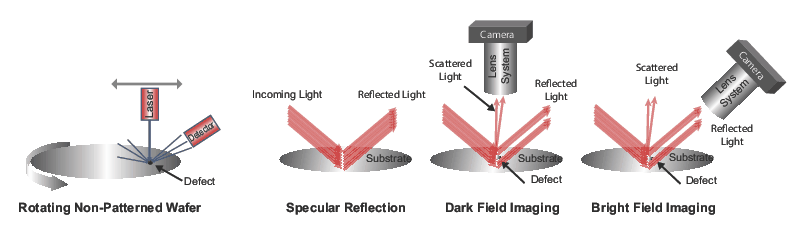
Inspecting Unpatterned Wafers

Kla Introduces Breakthrough Electron Beam Defect Inspection System
Over the years there have been tomes written about patterned wafer inspection.
Patterned wafer inspection system.
Semiconductor Inspection

Kla Tencor Announces Defect Inspection Systems News

Wafer Inspection System 390x Series Kla Tencor Surface Defect
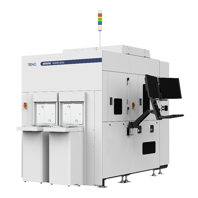
Wafer Inspection System Inspectra Series Optical Semiconductor Wafer Inspection System Product Information Tasmit Inc

Silicon Manufacturing How Wafers Are Inspected

Inspection System Zi 2000 Screen Semiconductor Solutions Co Ltd

Dark Field Wafer Defect Inspection System Is Series Hitachi High Tech Global

Optical Inspection System 8 Series Kla Tencor Scanning For Wafers Led

Optical Inspection Machine Puma 9980 Kla Tencor For Patterned Wafers Defect

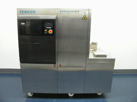
Kla Tencor Sfs 7600 Surfscan Patterned Wafer Inspection System Price Specs

Wafer Inspection Standards
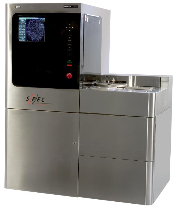
Kla Tencor Ait I Patterned Surface Defect Inspection System Classone Equipment

Wafer Surface Inspection System Ls Series Hitachi High Tech In America

Video 1 Kla Tencor 2139 Brightfield Patterned Wafer Inspection System Id 3735 Youtube
Source : pinterest.com
